|
Samsung Electronics Co., Ltd., the world leader in advanced memory technology, has recently developed the
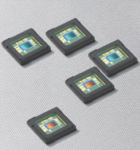
world first 1 GB (gigabit) mobile DRAM with a wide I/O interface, using 50 nanometer class process technology.
The new wide I/O mobile DRAM will be used in mobile applications, such as Smartphones and tablet PCs.
A senior vice president, memory product planning &application engineering at Samsung Electronics
announced that the company¡¯s new mobile DRAM solution with a wide I/O interface will be significantly
contributing to the advancement of high-performance mobile products following the development of 4GB LPDDR2
DRAM(lowpower DDR2 dynamic random access memory) last year.
He added that the company will further continue to aggressively expand its high-performance mobile memory
product line to further propel the growth of the mobile industry.
The new 1GB wide I/O mobile DRAM can transmit data at 12.8 gigabytes (GB) per second, which increases the
bandwidth of mobile DDR DRAM (1.6GB/s) eight-fold, thus reducing power consumption by approximately 87
percent. The bandwidth is also four times that of LPDDR2 DRAM-which is approximately 3.2GB/s).
To boost data transmission, the company¡¯s wide I/O DRAM uses 512 pins for data input and output compared
to the previous generation of mobile DRAMs, which employed a maximum of 32 pins. If users include the pins
that are involved in sending commands and regulating power supply, a single Samsung wide I/O DRAM can be
designed to accommodate approximately 1,200pins.
Samsung is further aiming to provide 20nm-class 4GB wide I/O mobile DRAM sometime in 2013, following this
wide I/O DRAM launch. The company¡¯s recent achievements in mobile DRAM include introducing the world
first 50nm-class 1Gb LPDDR2 DRAM in 2009 and the world first 40nm-class 2GB LPDDR2 in 2010.
According to iSuppli, a market research agency, mobile DRAM¡¯s percentage of total annual DRAM shipments
will be increasing from about 11.1 percent in 2010 to 16.5 percent in 2014.
|